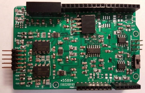
brain-duino parts Kit V0.2

Assemble instruction with Option A


==== ======== ======== ======== ======== ======== ======== ====
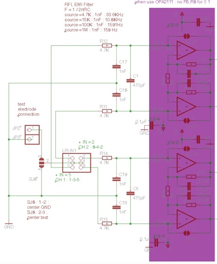
how to reduce noise from Bluetooth interface
======== ======== ======== ======== ======== ======== ======== ========
==================== end of assembled with Option A ============================================
in case all solder is ok as instruction then works.
connect 5V power to 5V pin ( Arduino pin name ), then check
followings voltage.
+12 V, - 12 V ( this will be max +- 5 % offset )
5 V external ref V ( Arduino pin name ).
SJ 7-R & SJ 8-R : offset Voltage 1.25 V.
AD 0 & AD 1 ( Arduino pin name ) : offset Voltage around 2.5 V ( this will be around +- 5 % offset ).
in case you have battery operated OSC then
connect it to input pin, then will have output
resolute to AD 0 & AD 1 pin.
use 0.1 Hz to 300 Hz OSC.
SW up position : 0.16 Hz .. 32 Hz
SW down position : 0.16 Hz .. 200 Hz
this frequency maybe +- 10 % difference.
see Option B setup :
http://www.psychiclab.net/IBVA/kit1-1.html
input resistance 1 K ohm to 1 M ohm and
p-p 5 µV to p-p 200 µV input to test.
OSC ground connect to GND.
connect OSC with resistance to CH1 + and CH1- input. then check output from AD 0.
connect OSC with resistance to CH2 + and CH2- input. then check output from AD 1.
check with Oscilloscope and/or after next step : construction, check with IBVA / BrainBay application.
this is one of idea for test amp noise from my instructables page.
http://www.instructables.com/id/open-brain-wave-interface-hardware-1/step10/amp-noise-test/
in case SJ6 and SJ7 open ( OFF ) then need to put two jumper
like this way.
then put OSC and resister instead of jumper can test electrode and skin contact condition.
6: solder Switch and connector
S2 DPDT IS-2235 switch-misc
1
JS202011CQN
VCC, GND, TXD, RXD 4 pin L-pinhead for BlueTooth
1
4 pin L plug : in case not L plug then bend it to L shape.
use for VCC, GND, TXD, RXD
IOH 1X10 pinhead Useconn Electronics
1
PINHD-1X10
10X1F-H8.5
IOL 1X08 pinhead Useconn Electronics
2
PINHD-1X8
8X1F-H8.5
POWER 1X08 pinhead Useconn Electronics
PINHD-1X8
8X1F-H8.5
AD 1X06 pinhead Useconn Electronics
1
PINHD-1X6
6X1F-H8.5
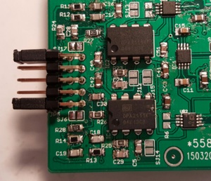
LR-IN1 2X05/90 pinhead
1
2X05 L pinhead
L & R brain wave input : input need to put center 2X03 position.
ICSP JP3Q jumper
3X2 M
1
SPI connection
Total : SJ X 16, C X 45, R X 35, Silicon chip X 12, SW X 1, Connector X 7,
solder like this :
solder like this :
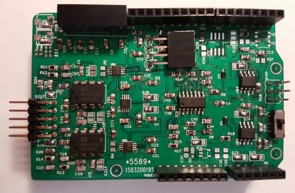
5: solder silicon chip
recommended to check with tester after each one solder
U$1 AD8422ARMZ MSOP MKH
2
AD8422ARMZ
< U$1, U$2 >
U$2 AD8422ARMZ MSOP MKH
AD8422ARMZ
IC1 OP2177ARMZ MSOP AD
1
OP2177ARMZ
< IC1 >
IC3 OP4177ARZ SO14 AD
1
OP4177ARZ
< IC3 >
U$4 MAX7480ESA+ MAX7480 MKH
2
MAX7480ESA+
< U$4, U$5 >
U$5 MAX7480ESA+ MAX7480 MKH
MAX7480ESA+
IC7 LT1761ES5-5 SOT23-5 v-reg-micrel LINEAR TEC
1
LT1761ES5-5
< IC7 >
U$7 DC-DC +-12V, RB-0512D/P MKH Recom Power
1
RB-0512D/P
< U$7 >
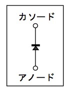
D1 ( UDZS5.1B ) SMB 5.1V zener diode ROHM
2
UDZSTE-175.1B : ( UDZS5.1B ) 5.1 V 2% 200mW 80 ohm, UMD2
< D1, D3 >
D3 ( UDZS5.1B ) SMB 5.1V zener diode ROHM
UDZSTE-175.1B : ( UDZS5.1B ) 5.1 V 2% 200mW 80 ohm, UMD2
solder like this :
Assembly variant:
Part Value Package Library
SJ1:1-2 :L SJ_2 jumper
default : SJ1:1-2 : +5 V from Arduino, SJ1:2-3 : 5.6..15V Direct input 200mA Max
SJ2:1-2 :L SJ_2 jumper
default : SJ2:1-2 when CH1:AD0, SJ2:2-3 when CH1:AD2
SJ3:1-2 :L SJ_2 jumper
default : SJ3:1-2 when CH2:AD1, SJ3:2-3 when CH2:AD3
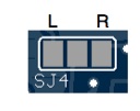
SJ4:2-3 :R SJ_2 jumper
default : SJ4:2-3, when use 555 or direct clock input use port D3 : SJ4:1-2
SJ5:2-3 :R SJ_2 jumper
default : SJ5:2-3, when use 555 or direct clock input use port D3 : SJ5:1-2
SJ6: jumper
default : ON
SJ7:2-3 :L SJ_2 jumper
default : SJ7:2-3 : Ref to GND, SJ7:1-2 : Ref to Ref V
SJ8:2-3 :L SJ_2 jumper
default : SJ8:2-3 : Ref to GND, SJ8:1-2 : Ref to Ref V
SJ9: NC SJ_2 jumper
default : SJ9:NC, when use 555 : SJ9:1-2, when direct clock input use port D3 : SJ9:2-3
SJ10, SJ11 jumper
default : ON
SJ12 jumper
default : OFF
when not use Option A then need to ON
SJ13 jumper
default : OFF
when not use Option A then need to ON
SJ14 jumper
default : OFF
when not use Option A then need to ON
SJ15 jumper
default : OFF
when not use Option A then need to ON
SJ16 jumper
default : ON
main board ( CH 1, CH 2 ) : ON
additional board ( CH 3, CH 4 ) : OFF
SJ17: jumper
default : ON
3: solder Capacitor
recommended to check with tester after each one solder
C1 470pF 5% C0805 rcl
6
470pF
< C1, 5 > < C24, C28, C29, C30 > Option A
C2 0.1µF C0805 rcl
18
0.1µF
< C2, 3, 4, 10, 12, 21, 22, 23, 27, 31, 40, 41, 42, 43, 48, 49, 50 51 >
C3 0.1µF C0805 rcl
C4 0.1µF C0805 rcl
C5 470pF C0805 rcl
C6 2.7nF 50V 5% (20KHz) 30ppm/degC C0805 rcl
2
2.7nF
< C6, 45 >
C8 10µF 25V 10% C0805 rcl
6
10µF
< C8, 9, 14, 20, 25, 26 >
C9 10µF C0805 rcl
C10 0.1µF C0805 rcl
C11 1µF 50V 10% C0805 rcl
2
1µF
< C11, 15 >
C12 0.1µF C0805 rcl
C13 15nF (+2.7nF=30Hz) 50V 5% 30ppm/degC C0805 rcl
2
15nF
< C13, 44 >
C14 10µF C0805 rcl
C15 1µF C0805 rcl
C16 1nF 5% C0805 rcl
4
1nF
< C16, 17, 18, 19 >
C17 1nF C0805 rcl
C18 1nF C0805 rcl
C19 1nF C0805 rcl
C20 10µF C0805 rcl
C21 0.1µF C0805 rcl
C22 0.1µF C0805 rcl
C23 0.1µF C0805 rcl
C24 470pF 5% C0805 rcl
C25 10µF C0805 rcl
C26 10µF C0805 rcl
C27 0.1µF C0805 rcl
C28 470pF 5% C0805 rcl
C29 470pF 5% C0805 rcl
C30 470pF 5% C0805 rcl
C31 0.1µF C0805 rcl
C32 0.01µF 10% C0805 rcl
1
0.01µF
< C32 >
C33 47pF 5% C0805 rcl
4
47pF
< C33, 34, 35, 36 >
C34 47pF C0805 rcl
C35 47pF C0805 rcl
C36 47pF C0805 rcl
C40 0.1µF C0805 rcl
C41 0.1µF C0805 rcl
C42 0.1µF C0805 rcl
C43 0.1µF C0805 rcl
C44 15nF (+2.7nF = 3KHz) 50V 5% 30ppm/degC C0805 rcl
C45 2.7nF 50V 5% (20KHz) 30ppm/degC C0805 rcl
C48 0.1µF C0805 rcl
C49 0.1µF C0805 rcl
C50 0.1µF C0805 rcl
C51 0.1µF C0805 rcl
4: solder Resistor
recommended to check with tester after each one solder
R1 1M 0.1% 25ppm/degC 0.1W R0805 rcl
8
1M
< R1, 2, 3, 4, 7, 8, 16, 19 >
R2 1M 0.1% 25ppm/degC 0.1W R0805 rcl
R3 1M 0.1% 25ppm/degC 0.1W R0805 rcl
R4 1M 0.1% 25ppm/degC 0.1W R0805 rcl
R5 200 0.1% 25ppm/degC 0.1W R0805 rcl
2
200 ohm
< R5, 6 >
R6 200 0.1% 25ppm/degC 0.1W R0805 rcl
R7 1M 0.1% 25ppm/degC 0.1W R0805 rcl
R8 1M 0.1% 25ppm/degC 0.1W R0805 rcl
R9 4.7K 1% 0.25W R0805 rcl
6
4.7K
< R9, 10, 11, 12, 13, 14 >
R10 4.7K 1% 0.25W R0805 rcl
R11 4.7K 1% 0.25W R0805 rcl
R12 4.7K 1% 0.25W R0805 rcl
R13 4.7K 1% 0.25W R0805 rcl
R14 4.7K 1% 0.25W R0805 rcl
R15 4.02K 0.1% 25ppm/degC 0.125W R0805 rcl
2
4.02K
< R15, 17 >
R16 1M 0.1% 25ppm/degC 0.1W R0805 rcl
R17 4.02K 0.1% 25ppm/degC 0.125W R0805 rcl
R18 470 5% 0.25W R0805 rcl
4
470 ohm
< R18, 20, 21, 38 >
R19 1M 0.1% 25ppm/degC 0.1W R0805 rcl
R20 470 5% 0.25W R0805 rcl
when use JY-MCU Bluetooth V1.0.6 then R20 to 0 ohm.
( V1.0.6 works with 5 V logic and 5 V power, before then 3.3 V logic with 5 V power. R20 use for it. )
R21 470 5% 0.25W R0805 rcl
R22 1K 1% 0.25W R0805 rcl
2
1K
< R22, 33 >. when use JY-MCU Bluetooth V1.0.6 then no need R22.
( V1.0.6 works with 5 V logic and 5 V power, before then 3.3 V logic with 5 V power. R22 use for it. )
R23 100K 0.1% 25ppm/degC 0.125W R0805 rcl
4
100K
< R23, R24, R25, R26 > option A
R24 100K 0.1% 25ppm/degC 0.125W R0805 rcl
R25 100K 0.1% 25ppm/degC 0.125W R0805 rcl
R26 100K 0.1% 25ppm/degC 0.125W R0805 rcl
R27 2K 0.1% 25ppm/degC 0.125W R0805 rcl
2
2K
< R27, R28 > option A
R28 2K 0.1% 25ppm/degC 0.125W R0805 rcl
R29 2.15K 0.1% 25ppm/degC 0.125W R0805 rcl
2
2.15K
< R29 & R34: 1-3 >
R33 1K 1% 0.25W R0805 rcl
R34 SJ11 ON and put 2.15K at 1-3
R35 SJ10 ON
R38 470 5% 0.25W R0805 rcl
R39 4.3K 0.1% 25ppm/degC 0.125W R0805 rcl
1
4.3K
<R39>
SJ10 & SJ11 ON : set 1.25V offset,
default : SJ10 & SJ11 ON : set 1.25V offset,
0 ohm at C46 & C47 for no DC cut
2
0 ohm
default : 0 ohm at C46 & C47 for no DC cut
( R 2.15K at R34: 2-1, R 0 ohm at R34:2-3 & R35:2-3 : set 2.5V offset )
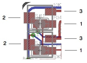
2: solder jumper
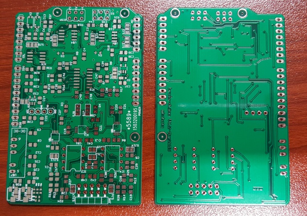
SJ : solder jumper connection : view PCB this way.
L mean connect L and center, R mean connect R and center, NC mean none connection
Up mean connect Up and center
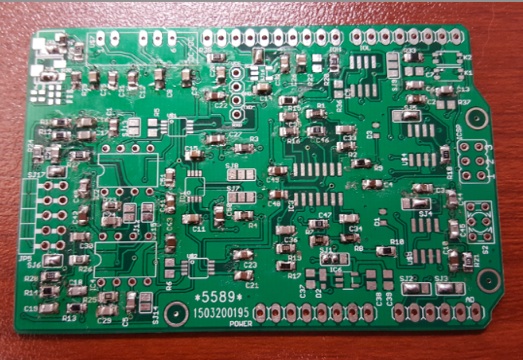
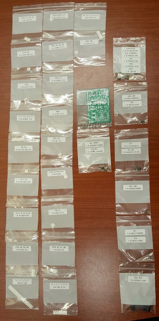
1: check all parts
PCB bag X 1, SW & connector bag X 2, IC bag X 5, C bag X 9, R bag X 11
Total : C X 45, R X 35, Silicon chip X 12, SW X 1, Connector X 7, PCB X 1
actual shipment maybe different package.
assemble time will be 4 .. 8 hours. in case no mistake.
=======
Parts List V0.2 : March 2015